- 您现在的位置:买卖IC网 > Sheet目录1999 > IDT2308A-4DCI8 (IDT, Integrated Device Technology Inc)IC CLOCK MULT ZD HI DRV 16-SOIC
1
COMMERCIALANDINDUSTRIALTEMPERATURERANGES
IDT2308A
3.3V ZERO DELAY CLOCK MULTIPLIER
AUGUST 2012
2012
Integrated Device Technology, Inc.
DSC 6587/9
c
COMMERCIAL AND INDUSTRIAL TEMPERATURE RANGES
The IDT logo is a registered trademark of Integrated Device Technology, Inc.
FEATURES:
Phase-Lock Loop Clock Distribution for Applications ranging
from 10MHz to 133MHz operating frequency
Distributes one clock input to two banks of four outputs
Separate output enable for each output bank
External feedback (FBK) pin is used to synchronize the outputs
to the clock input
Output Skew <200 ps
Low jitter <200 ps cycle-to-cycle
1x, 2x, 4x output options (see table):
– IDT2308A-1 1x
– IDT2308A-2 1x, 2x
– IDT2308A-3 2x, 4x
– IDT2308A-4 2x
– IDT2308A-1H and -2H for High Drive
No external RC network required
Operates at 3.3V VDD
Available in SOIC and TSSOP packages
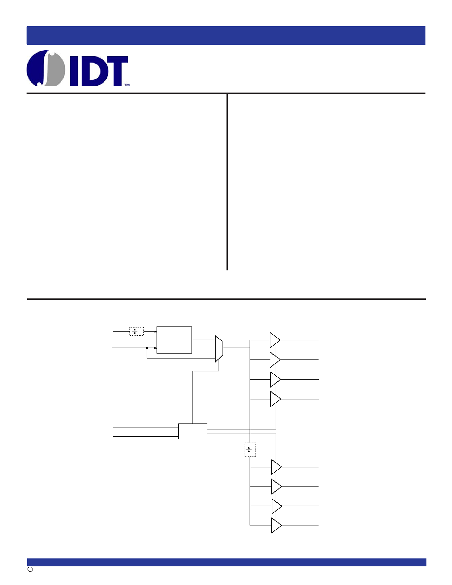
FUNCTIONALBLOCKDIAGRAM
DESCRIPTION:
The IDT2308A is a high-speed phase-lock loop (PLL) clock multiplier. It is
designedtoaddresshigh-speedclockdistributionandmultiplicationapplica-
tions.Thezerodelayisachievedbyaligningthephasebetweentheincoming
clock and the output clock, operable within the range of 10 to 133MHz.
TheIDT2308Ahastwobanksoffouroutputseachthatarecontrolledviatwo
selectaddresses.Byproperselectionofinputaddresses,bothbankscanbe
put in tri-state mode. In test mode, the PLL is turned off, and the input clock
directly drives the outputs for system testing purposes. In the absence of an
input clock, the IDT2308A enters power down. In this mode, the device will
drawlessthan12AforCommercialTemperaturerangeandlessthan25A
forIndustrialtemperaturerange,andtheoutputsaretri-stated.
The IDT2308A is available in six unique configurations for both pre-
scaling and multiplication of the Input REF Clock. (See available options
table.)
ThePLLisclosedexternallytoprovidemoreflexibilitybyallowingtheuser
tocontrolthedelaybetweentheinputclockandtheoutputs.
TheIDT2308AischaracterizedforbothIndustrialandCommercialopera-
tion.
IDT2308A
3.3V ZERO DELAY CLOCK
MULTIPLIER
PLL
S1
2
14
15
3
CLKA1
CLKA2
CLKA3
CLKA4
6
10
11
CLKB1
CLKB2
CLKB3
CLKB4
9
FBK
16
Control
Logic
7
8
1
REF
S2
(-2, -3)
(-3, -4)
2
发布紧急采购,3分钟左右您将得到回复。
相关PDF资料
IDT2309-1HPGGI
IC CLK BUFFER ZD HI DRV 16-TSSOP
IDT2309A-1HPGG
IC CLK BUFFER ZD HI DRV 16-TSSOP
IDT2309B-1HPGGI
IC CLK BUFFER HIGH DRIVE 16TSSOP
IDT23S05-1HDCGI
IC CLK BUFFER PLL HI DRV 8-SOIC
IDT23S05E-1HDCGI8
IC CLK BUFFER PLL HI DRV 8-SOIC
IDT23S08-1HPGI8
IC CLK MULT PLL HI DRV 16-TSSOP
IDT23S08T-1DC
IC CLK MULT PLL ZD 2.5V 16-SOIC
IDT23S09T-1DC8
IC CLK BUFFER ZD 2.5V 16-SOIC
相关代理商/技术参数
IDT2308A-4PG
制造商:IDT 制造商全称:Integrated Device Technology 功能描述:3.3V ZERO DELAY CLOCK MULTIPLIER
IDT2308A-4PGG
制造商:IDT 制造商全称:Integrated Device Technology 功能描述:3.3V ZERO DELAY CLOCK MULTIPLIER
IDT2308A-4PGGI
制造商:IDT 制造商全称:Integrated Device Technology 功能描述:3.3V ZERO DELAY CLOCK MULTIPLIER
IDT2308A-4PGI
制造商:IDT 制造商全称:Integrated Device Technology 功能描述:3.3V ZERO DELAY CLOCK MULTIPLIER
IDT2308A-5HDC
功能描述:IC CLOCK MULT ZD HI DRV 16-SOIC RoHS:否 类别:集成电路 (IC) >> 时钟/计时 - 时钟发生器,PLL,频率合成器 系列:- 产品变化通告:Product Discontinuation 04/May/2011 标准包装:96 系列:- 类型:时钟倍频器,零延迟缓冲器 PLL:带旁路 输入:LVTTL 输出:LVTTL 电路数:1 比率 - 输入:输出:1:8 差分 - 输入:输出:无/无 频率 - 最大:133.3MHz 除法器/乘法器:是/无 电源电压:3 V ~ 3.6 V 工作温度:0°C ~ 70°C 安装类型:表面贴装 封装/外壳:16-TSSOP(0.173",4.40mm 宽) 供应商设备封装:16-TSSOP 包装:管件 其它名称:23S08-5HPGG
IDT2308A-5HDC8
功能描述:IC CLOCK MULT ZD HI DRV 16-SOIC RoHS:否 类别:集成电路 (IC) >> 时钟/计时 - 时钟发生器,PLL,频率合成器 系列:- 产品变化通告:Product Discontinuation 04/May/2011 标准包装:96 系列:- 类型:时钟倍频器,零延迟缓冲器 PLL:带旁路 输入:LVTTL 输出:LVTTL 电路数:1 比率 - 输入:输出:1:8 差分 - 输入:输出:无/无 频率 - 最大:133.3MHz 除法器/乘法器:是/无 电源电压:3 V ~ 3.6 V 工作温度:0°C ~ 70°C 安装类型:表面贴装 封装/外壳:16-TSSOP(0.173",4.40mm 宽) 供应商设备封装:16-TSSOP 包装:管件 其它名称:23S08-5HPGG
IDT2308A-5HDCI
功能描述:IC CLOCK MULT ZD HI DRV 16-SOIC RoHS:否 类别:集成电路 (IC) >> 时钟/计时 - 时钟发生器,PLL,频率合成器 系列:- 产品变化通告:Product Discontinuation 04/May/2011 标准包装:96 系列:- 类型:时钟倍频器,零延迟缓冲器 PLL:带旁路 输入:LVTTL 输出:LVTTL 电路数:1 比率 - 输入:输出:1:8 差分 - 输入:输出:无/无 频率 - 最大:133.3MHz 除法器/乘法器:是/无 电源电压:3 V ~ 3.6 V 工作温度:0°C ~ 70°C 安装类型:表面贴装 封装/外壳:16-TSSOP(0.173",4.40mm 宽) 供应商设备封装:16-TSSOP 包装:管件 其它名称:23S08-5HPGG
IDT2308A-5HDCI8
功能描述:IC CLOCK MULT ZD HI DRV 16-SOIC RoHS:否 类别:集成电路 (IC) >> 时钟/计时 - 时钟发生器,PLL,频率合成器 系列:- 产品变化通告:Product Discontinuation 04/May/2011 标准包装:96 系列:- 类型:时钟倍频器,零延迟缓冲器 PLL:带旁路 输入:LVTTL 输出:LVTTL 电路数:1 比率 - 输入:输出:1:8 差分 - 输入:输出:无/无 频率 - 最大:133.3MHz 除法器/乘法器:是/无 电源电压:3 V ~ 3.6 V 工作温度:0°C ~ 70°C 安装类型:表面贴装 封装/外壳:16-TSSOP(0.173",4.40mm 宽) 供应商设备封装:16-TSSOP 包装:管件 其它名称:23S08-5HPGG